17.5.23
Article: Coherent imaging and dynamics of excitons in MoSe2 monolayers epitaxially grown on hexagonal boron nitride
The technology of preparing heterostructures made of semiconducting transition metal dichalcogenides (TMDs) is based on the exfoliation of thin films from van der Waals bulk crystals. While the nonscalability of the exfoliation top-down approach is not an issue in the fundamental research, for which the proof-of-principle demonstrations are essential, it is a major roadblock on the academia-industry pathway of this field. In order to merge these novel materials with the semiconductor microelectronics, strain-free monolayer samples homogeneously covering wafers of a few-inch diameter are required.
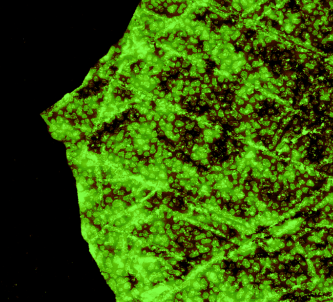
Here we present studies of MoSe2 grown by molecular beam epitaxy on the silicon substrate with exfoliated hBN flakes. We performed four-wave-mixing (FWM) imaging and spatially correlated the obtained amplitude of the nonlinear optical response of the studied flakes with the layer thickness obtained from AFM measurements. It allowed us to precisely characterize the signal originating from the epitaxially-grown monolayers with respect to the surface morphology. Furthermore, by measuring the FWM signal in the temporal domain we were able to determine the dephasing dynamics of exciton complexes and ascertained their temperature dependence.
Our results show that these epitaxial monolayers, while opening the prospect of being compatible with the semiconductor optoelectronics industry, display excellent optical response, providing they crystalize on atomically flat surfaces, here provided by hBN flakes. The quality and intensity of the produced signal are comparable with their non-encapsulated counterparts obtained via exfoliation. As such, our findings fortify the viability of the MBE growth method for the production of high-quality TMD monolayers. Furthermore, its inherent versatility opens up alluring new research venues for this particular family of 2D materials.
Authors: Karolina Ewa Połczyńska, Simon Le Denmat, Takashi Taniguchi, Kenji Watanabe, Marek Potemski, Piotr Kossacki, Wojciech Pacuski and Jacek Kasprzak
Nanoscale, 2023,15, 6941-6946
Published 21 March 2023
https://doi.org/10.1039/D2NR04844B
